LTC1704/LTC1704B
12
1704bfa
APPLICATIO S I FOR ATIO
U
U
U
In combination with a simple external charge pump (Fig-
ure 2), this allows the LTC1704 to completely enhance the
gate of QT without requiring an additional, higher supply
voltage.
Switcher Supply Feedback Amplifier
The LTC1704 senses the switcher output voltage at V
OUTSW
with an internal feedback op amp (see Block Diagram).
This is a real op amp with a low impedance output, 85dB
open-loop gain and 20MHz gain bandwidth product. The
positive input is connected internally to an 800mV refer-
ence, while the negative input is connected to the FB pin.
The output is connected to COMP, which is in turn con-
nected to the soft-start circuitry and from there to the
PWM generator. The switching regulator output voltage
can be obtained using the following equation:
V
V
R
R
OUTSW
=
+
?/DIV>
?/DIV>
?/DIV>
?/DIV>
?/DIV>
?/DIV>
08 1
1
2
. "
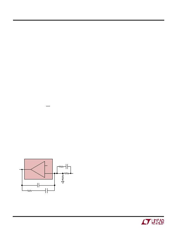
Unlike many regulators that use a resistor divider con-
nected to a high impedance feedback input, the LTC1704
switcher supply is designed to use an inverting summing
amplifier topology with the FB pin configured as a virtual
ground. This allows flexibility in choosing pole and zero
locations not available with simple g
m
configurations. In
particular, it allows the use of
Type 3
compensation,
which provides a phase boost at the LC pole frequency
and significantly improves loop phase margin (refer to
Figure3).
Switcher Supply MIN/MAX Comparators
Two additional feedback loops in the switcher supply keep
an eye on the primary feedback amplifier and step in if the
feedback node moves ?% from its nominal 800mV value.
The MAX comparator (see Block Diagram) activates when-
ever FB rises more than 5% above 800mV. It immediately
turns the top MOSFET (QT) off and the bottom MOSFET
(QB) on and keeps them that way until FB falls back within
5% of its nominal value. This pulls the output down as fast
as possible, preventing damage to the (often expensive)
load. If FB rises because the output is shorted to a higher
supply, QB will stay on until the short goes away, the
higher supply current limits or QB dies trying to save the
load. This behavior provides maximum protection against
overvoltage faults at the output, while allowing the circuit
to resume normal operation when the fault is removed.
The MIN comparator (see Block Diagram) trips whenever
FB is more than 5% below 800mV and immediately forces
the switch duty cycle to 90% to bring the output voltage
back into range. It releases when FB is within the 5%
window. MIN is disabled when the soft-start or current
limit circuits are activethe only two times that the output
should legitimately be below its regulated value.
Notice that the FB pin is the virtual ground node of the
feedback amplifier. A typical compensation network does
not include local DC feedback around the amplifier, so that
the DC level at FB will be an accurate replica of the output
voltage, divided down by R1 and R2 (Figure 3). However,
the compensation capacitors will tend to attenuate AC
signals at FB, especially with low bandwidth Type 1 feed-
back loops. This creates a situation where the MIN and
MAX comparators do not respond immediately to shifts in
the output voltage, since they monitor the output at FB.
PGOOD Flag
The LTC1704 comes with a power good pin (PGOOD).
PGOOD is an open-drain output, and requires an external
pull-up resistor. If both the regulators are within ?0%
from their nominal value, the transistor MPG shuts off (see
Block Diagram), and PGOOD is pulled high by the external
pull-up resistor. If any of the two outputs is more than 10%
outside the nominal value for more than 1祍, PGOOD pulls
Figure 3. "Type 3" Feedback Loop
+
FB
0.8V
R1
FB
V
OUTSW
LTC1704
COMP
1704 F03
R3
C3
C2
R2
R4
C1
发布紧急采购,3分钟左右您将得到回复。
相关PDF资料
LTC1966MPMS8#TRPBF
IC RMS/DC CONV MICROPWR 8-MSOP
LTC1967IMS8#TRPBF
IC CONVERTER RMS-DC PREC 8MSOP
LTC1968IMS8#TRPBF
IC CONVERTER RMS-DC PREC 8MSOP
LTC3100EUD#TRPBF
IC REG BUCK/BOOST/LINEAR 16-QFN
LTC3104IMSE#TRPBF
IC REG DL BCK/LINEAR SYNC 16MSOP
LTC3445EUF#TRPBF
IC REG TRPL BUCK/LINEAR 24-QFN
LTC3446IDE#PBF
IC REG TRPL BCK/LINEAR 14-DFN
LTC3537EUD#TRPBF
IC REG DL BST/LINEAR SYNC 16-QFN
相关代理商/技术参数
LTC1705EGN
功能描述:IC PWR SUPPLY CONTROLLER 28SSOP RoHS:否 类别:集成电路 (IC) >> PMIC - 电源控制器,监视器 系列:- 产品培训模块:Lead (SnPb) Finish for COTS
Obsolescence Mitigation Program 标准包装:2,500 系列:- 应用:多相控制器 输入电压:- 电源电压:9 V ~ 14 V 电流 - 电源:- 工作温度:-40°C ~ 85°C 安装类型:表面贴装 封装/外壳:40-WFQFN 裸露焊盘 供应商设备封装:40-TQFN-EP(5x5) 包装:带卷 (TR)
LTC1705EGN#PBF
功能描述:IC PWR SUPPLY CONTROLLER 28SSOP RoHS:是 类别:集成电路 (IC) >> PMIC - 电源控制器,监视器 系列:- 产品培训模块:Lead (SnPb) Finish for COTS
Obsolescence Mitigation Program 标准包装:2,500 系列:- 应用:多相控制器 输入电压:- 电源电压:9 V ~ 14 V 电流 - 电源:- 工作温度:-40°C ~ 85°C 安装类型:表面贴装 封装/外壳:40-WFQFN 裸露焊盘 供应商设备封装:40-TQFN-EP(5x5) 包装:带卷 (TR)
LTC1705EGN#TR
功能描述:IC PWR SUPPLY CONTROLLER 28SSOP RoHS:否 类别:集成电路 (IC) >> PMIC - 电源控制器,监视器 系列:- 产品培训模块:Lead (SnPb) Finish for COTS
Obsolescence Mitigation Program 标准包装:2,500 系列:- 应用:多相控制器 输入电压:- 电源电压:9 V ~ 14 V 电流 - 电源:- 工作温度:-40°C ~ 85°C 安装类型:表面贴装 封装/外壳:40-WFQFN 裸露焊盘 供应商设备封装:40-TQFN-EP(5x5) 包装:带卷 (TR)
LTC1705EGN#TRPBF
功能描述:IC PWR SUPPLY CONTROLLER 28SSOP RoHS:是 类别:集成电路 (IC) >> PMIC - 电源控制器,监视器 系列:- 产品培训模块:Lead (SnPb) Finish for COTS
Obsolescence Mitigation Program 标准包装:2,500 系列:- 应用:多相控制器 输入电压:- 电源电压:9 V ~ 14 V 电流 - 电源:- 工作温度:-40°C ~ 85°C 安装类型:表面贴装 封装/外壳:40-WFQFN 裸露焊盘 供应商设备封装:40-TQFN-EP(5x5) 包装:带卷 (TR)
LTC1706CS8-19
功能描述:IC VID VOLTAGE PROGRAMMER 8SOIC RoHS:否 类别:集成电路 (IC) >> PMIC - 电源控制器,监视器 系列:- 产品培训模块:Lead (SnPb) Finish for COTS
Obsolescence Mitigation Program 标准包装:2,500 系列:- 应用:多相控制器 输入电压:- 电源电压:9 V ~ 14 V 电流 - 电源:- 工作温度:-40°C ~ 85°C 安装类型:表面贴装 封装/外壳:40-WFQFN 裸露焊盘 供应商设备封装:40-TQFN-EP(5x5) 包装:带卷 (TR)
LTC1706CS8-19#PBF
功能描述:IC VID VOLTAGE PROGRAMMER 8SOIC RoHS:是 类别:集成电路 (IC) >> PMIC - 电源控制器,监视器 系列:- 产品培训模块:Lead (SnPb) Finish for COTS
Obsolescence Mitigation Program 标准包装:2,500 系列:- 应用:多相控制器 输入电压:- 电源电压:9 V ~ 14 V 电流 - 电源:- 工作温度:-40°C ~ 85°C 安装类型:表面贴装 封装/外壳:40-WFQFN 裸露焊盘 供应商设备封装:40-TQFN-EP(5x5) 包装:带卷 (TR)
LTC1706CS8-19#TR
功能描述:IC VID VOLTAGE PROGRAMMER 8SOIC RoHS:否 类别:集成电路 (IC) >> PMIC - 电源控制器,监视器 系列:- 产品培训模块:Lead (SnPb) Finish for COTS
Obsolescence Mitigation Program 标准包装:2,500 系列:- 应用:多相控制器 输入电压:- 电源电压:9 V ~ 14 V 电流 - 电源:- 工作温度:-40°C ~ 85°C 安装类型:表面贴装 封装/外壳:40-WFQFN 裸露焊盘 供应商设备封装:40-TQFN-EP(5x5) 包装:带卷 (TR)
LTC1706CS8-19#TRPBF
功能描述:IC VID VOLTAGE PROGRAMMER 8SOIC RoHS:是 类别:集成电路 (IC) >> PMIC - 电源控制器,监视器 系列:- 产品培训模块:Lead (SnPb) Finish for COTS
Obsolescence Mitigation Program 标准包装:2,500 系列:- 应用:多相控制器 输入电压:- 电源电压:9 V ~ 14 V 电流 - 电源:- 工作温度:-40°C ~ 85°C 安装类型:表面贴装 封装/外壳:40-WFQFN 裸露焊盘 供应商设备封装:40-TQFN-EP(5x5) 包装:带卷 (TR)